Corning
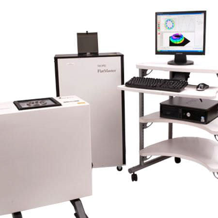
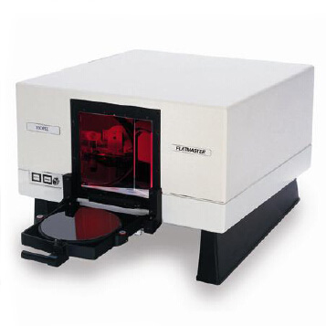
Tropel® FlatMaster® System
The Tropel® FlatMaster® provides industry-leading performance of surface form measurements for precision-component manufacturers. Our non-contact optical technique records the entire surface in seconds.
The FlatMaster® offers five-nanometer resolution and a standard accuracy of 50 nanometers (2.0 µ“). It rapidly and accurately measures flatness, line profile, radius, and other surface parameters from a variety of surfaces.
Several standard versions of the FlatMaster® are available to optimize accuracy over different component size ranges. The FlatMaster® 40, 100, and 200 measures parts up to 40 mm, 100 mm, and 200 mm respectively.
Customizing is available to achieve your specific performance requirements whether it is for increasing dynamic range, accuracy, or to include component handling features.
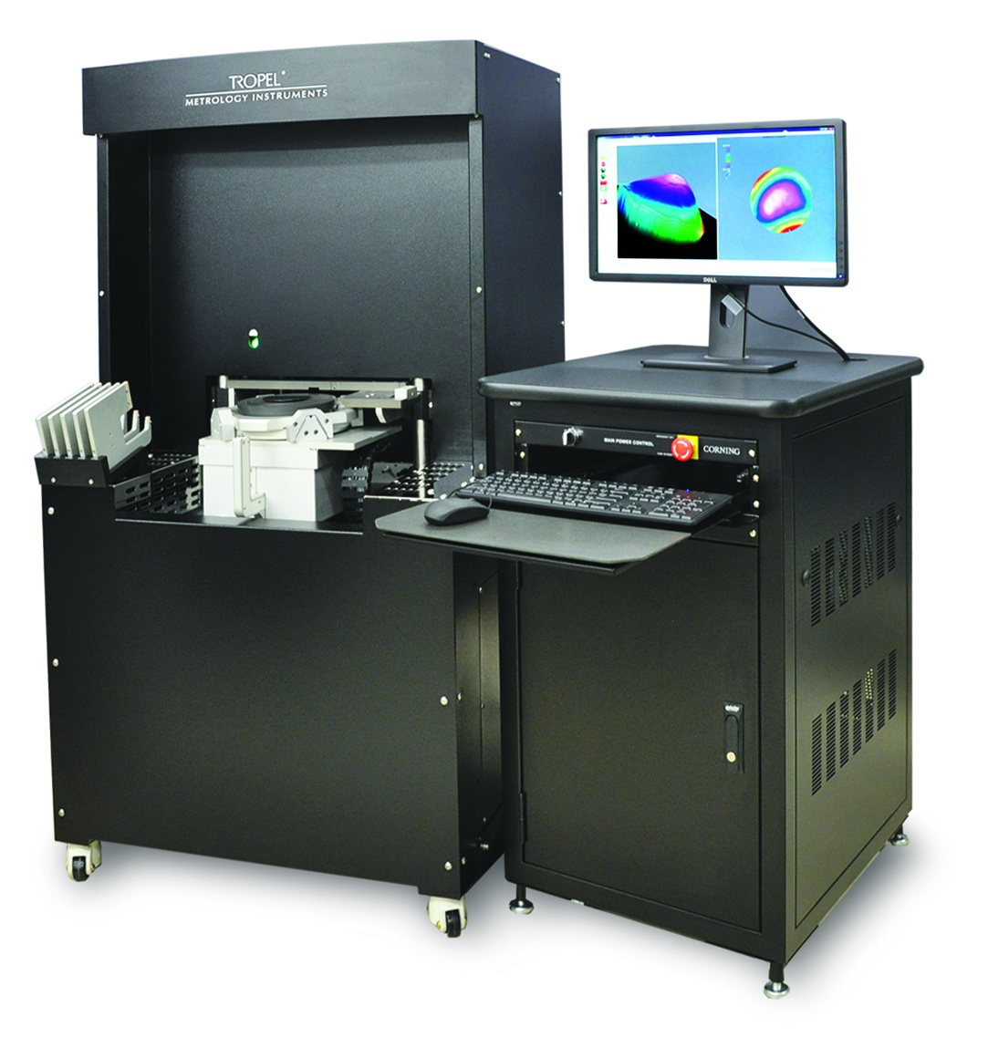
Tropel® FlatMaster® MSP
The Tropel® FlatMaster® MSP (Multi-Surface Profiler) is a frequency stepping interferometer that provides fast and accurate metrology for semiconductor wafers up to 300mm in diameter. In seconds up to 3 million data points are collected with sub-micron accuracy enabling total thickness and flatness characterization over the entire surface.
The FlatMaster® MSP provides robust metrology for a variety of applications from complex components and assemblies to transparent materials and wafer metrology. The FlatMaster MSP-DH is configured to simultaneously measure two sides of a component or assembly providing absolute thickness and parallelism measurements.
The ability to measure flatness, thickness, and thickness variation of 300 millimeter glass and silicon wafers is critical for successful integration of 3DIC assemblies. Traditional contact probes or conventional interferometry systems are too slow or do not have the necessary accuracy for larger fields of view.
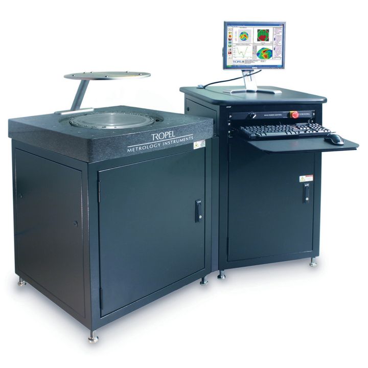
Corning Tropel® UltraFlat 200 Mask System
®
The Tropel® UltraFlatTM 200 Mask System was designed specifically for the photomask industry. It delivers the lowest measurement uncertainty for ever-tightening mask flatness specifications. Shrinking device features require not only flatter wafers, but flatter masks.
The UltraFlatTM system is used to measure flatness of photoblanks and photomasks throughout every stage of manufacturing and use, including substrate polishing, coating and patterning to analyze film stress, and verification.
The UltraFlatTM system utilizes near-normal incidence interferometry, rock-solid structural design, state-of-the-art optical fabrication techniques and Tropel’s renowned phase-shifting analysis software to deliver 20 nanometer measurement uncertainty.
The system is National Institute of Standards and Technology (NIST)-traceable and provides measurements that conform to SEMI standards. An automated photomask handling and measurement configuration is also available.
Tropel® Wafer Analysis Systems
Corning Specialty Materials has a long heritage of providing solutions to semiconductor equipment manufacturers. The Tropel line of wafer analysis equipment enables measurement of wafer substrates from 2” to 450mm regardless of material type and surface finish.
The continued demand for higher-density chips with smaller critical dimensions leads to tighter substrate form tolerances both on the global scale and on the individual die-site scale. Corning Tropel® has optimized our patented interferometry technologies for the highest-precision wafer flatness measurements. From wire saw to finished wafer, you can quickly and accurately measure wafer topography to verify that you or your customers have the ability to achieve the required device yields.
All Tropel® wafer systems measure flatness, taper, thickness variation, thickness, stress, bow, warp, SORI, and all SEMI standard parameters including stepper simulation of any wafer surface.
FlatMaster® Wafer System
The FlatMaster® Wafer System is ideal for processes development, regardless of material type. Combined with our state-of-the-art optical fabrication techniques and Tropel’s renowned phase-shifting analysis software, the FlatMaster Wafer system offers full-form surface information with 50 nanometer accuracy in seconds.
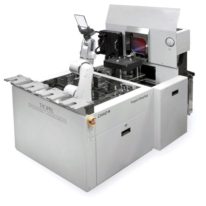
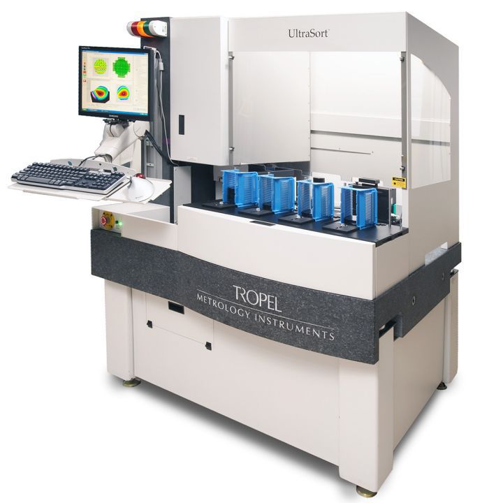
The Tropel® UltaSortTM
The Tropel® UltraSortTM is a fully automated, non-contact metrology tool designed for fast and accurate measurement of semiconductor wafers ranging in sizes from 2 inches to 8 inches in diameter. The user-configurable menu software allows the operator to define the sorting criteria via cassette-to-cassette wafer handling.
The UltraSort is capable of measuring a variety of materials including silicon, gallium arsenide, sapphire, quartz, germanium, Silicon Carbide and others. This Class 100 cleanroom-compliant system integrates a grazing-incidence interferometer with industry-standard robotic handling.
Contact us
Location
Max-Eyth Straße 46
73479 Ellwangen
Germany